ANKER Mini 30W GaN PD Charger A2147 Teardown
ID: 160191
Description: Anker has launched a new second-generation...
Steps:
- The packaging box design is simple, with the ANKER brand and SERIES 5 printed on the front.
- Product parameter information is printed on the back sticker.
- The package contains the charger, instruction manual, product certificate, etc.
- The charger is purple, the main shell has a frosted, anti-fingerprint finish, and the top is embedded with a transparent decorative panel, giving it an overall exquisite and beautiful appearance.
- The charger specifications are printed on the bottom shell: Model: A2147; Input: 100-240V~50/60Hz 1A; Output: 5V3A, 9V3A, 15V2A, 20V1.5A; PPS: 3.3-11V3A, 3.3-16V2A; Anker Innovation Technology Co., Ltd. The charger has passed CCC certification.
- The charger is equipped with foldable national standard pins, making it very convenient to take out for use.
- In addition to the decorative panel, the top surface is also designed with the ANKER brand and the IQ³ fast charging logo.
- There is a single USB-C port on the edge, with a classic blue plastic core.
- 测得机身高度为 35.52 mm。
- 宽度为 28.49 mm。
- 宽度为 28.46 mm。
- Compared with the Apple 30W charger, the size advantage is obvious.
- It feels intuitive in the hand—small and exquisite.
- In addition, the measured net weight of the charger is about 38 g.
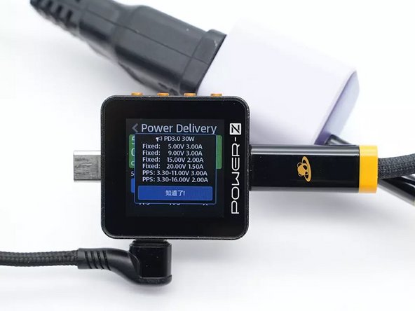
- Using the ChargerLAB POWER-Z KM002C, the charger supports the FCP, AFC, PD3.0, PPS, and QC4 charging protocols.
- In addition, it also has four fixed voltage gear sets of 5V3A, 9V3A, 15V2A, and 20V1.5A, and two PPS voltage gear sets of 3.3-11V3A and 3.3-16V2A.
- After reading the unboxing and testing of Anker's 30W GaN charger, let’s move on to the disassembly process to take a look at the internal components and design of this charger.
- 沿着充电器插脚侧的接缝处进行拆解,并取下折叠式插脚。
- 折叠式插脚上贴有用于绝缘的聚酯薄膜 (mylar) 片。
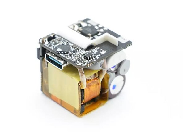
- The PCBA module is composed of two PCBs welded together.
- The bottom board is welded with the rectifier bridge, synchronous rectification circuit and protocol chip, and the primary and secondary stages are isolated and insulated with white plastic brackets.
- The small side board is welded with gallium nitride packaged chips, transformers and high-voltage filter capacitors to make full use of the space.
- The space between the two PCBs is soldered with high-voltage filter capacitors and transformers.
- Separate the two small boards by welding, and use a white plastic insulator between the small boards for isolation between the primary electrolytic capacitor and the output solid capacitor.
- Through the observation of the charger PCBA module, it is found that Anker's 30W GaN charger adopts a high-frequency QR switching power supply design, uses Nanxin Technology to seal the GaN chip and synchronous rectification controller, and the output voltage is passed by the protocol chip. Optocoupler control.
- Next, we will start to understand the design and materials of the entire charger from the input end.
- Front view of the small board at the bottom, welding fuse, common mode inductor, synchronous rectifier, VBUS switch tube and USB-C socket. The output filter capacitor is welded by sinking plate to reduce the thickness.
- The rectifier bridge, protocol chip and synchronous rectification controller are welded on the back of the small board.
- The time-delay fuse at the input end comes from Beite Electronics, and its specification is 2A 250V.
- The common mode inductor is wound with enameled wire and insulated wire, and wrapped with high temperature tape for insulation.
- The rectifier bridge comes from ZOWIE Zhiwei, model Z4RGP30MP, it is a fast recovery rectifier bridge, the specification is 1000V 3A, it adopts SMD package.
- The pulsating direct current output by the rectifier bridge is connected to the small side board, and is filtered by an electrolytic capacitor to supply power to the GaN packaged chip.
- The front side of the small side board is welded with differential mode inductors, filter electrolytic capacitors and transformers.
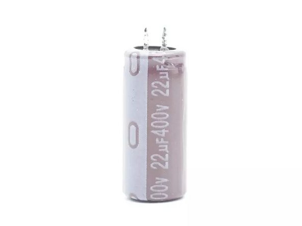
- The two high-voltage filter capacitors are from YMIN, and one of them has a specification of 33μF400V.
- The other specification is 22μF400V.
- The differential mode inductor is wound with an I-shaped magnetic core, and the jacket is insulated with a heat-shrinkable tube.
- The switching power supply's main control chip uses the Nanxin Technology SC3056, which features an integrated gallium nitride power device and controller.
- A 300 mΩ resistor is used to sense the primary current.
- The transformer uses an EE15 bobbin, with the magnetic core wrapped in copper foil for shielding and an outer layer of high-temperature tape for insulation.
- SMD Y capacitors are from Anshan Qifa.
- SMD optocoupler is used for output voltage feedback regulation.
- The synchronous rectification controller comes from Nanxin Technology, model SC3503, which is an adaptive turn-on detection and fast turn-off synchronous rectification controller.
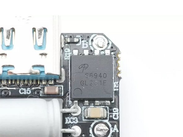
- Synchronous rectification MOS tube screen printing 66940, from AOS Bandai.
- The output filter capacitor is from YMIN, NPX series solid capacitor, the specification is 470μF 25V.
- The USB PD fast charging protocol chip adopts Infineon CYPD3174, which supports PD3.0 including PPS protocol, QC4.0, Apple 2.4A and other fast charging protocols; built-in multiple comprehensive protection functions, built-in 32-bit M0 processor, Integrated oscillator and no external clock required.
- Weld an NTC thermistor on the left side of CYPD3174 to detect the internal temperature of the USB-C socket and the charger to realize the live protection function.
- The USB-C female seat uses blue rubber core, and is fixed by through-hole welding.
- All disassembled
- Dismantling summary Anker's second-generation Anxin Charger 511 has a built-in sealed gallium nitride chip, an upgraded output power to 30W, and a built-in folding pin, which is compact and easy to carry.
- The charger has a variety of colors, and you can choose the MFI data cable of the same color as the charger, which is more personalized. In addition to being able to charge Apple users at full speed, it can also charge laptops, and supports PPS fast charging, and the fast charging compatibility with Android phones is also good.
- Through dismantling, we learned that this charger is internally welded with two PCBs, and a plastic bracket is used for primary and secondary insulation. Built-in Nanxin Technology's packaged GaN power solution, using SC3056 packaged GaN chip with SC3503 synchronous rectification controller.
- The protocol chip uses Infineon CYPD3174, and the primary electrolytic capacitor and output filter capacitor are from YMIN. The internal design is compact and the workmanship is solid.