Fnirsi FNB58 USB tester Teardown
ID: 169744
Description:
Steps:
- Start with the back side and use a TR6 bit to remove the four screws (circled in red).
- Remove first cover by carefully prying (e.g. with an old (credit) card)
- It should not take much force
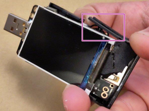
- In the created opening, roughly where the red square marking is, there is a small plastic latch/hook.
- Lightly press it down and pry on the back cover with the bluetooth logo.
- This is the hardest step. Be patient and careful.
- There is two more latches/hooks, these should not pose a big problem once the first one came lose.
- Carefully slide out the electronics.
- You can see a screen on a PCB in a black plastic frame.
- Remove the PCB from the frame
- Remove the black foam tape
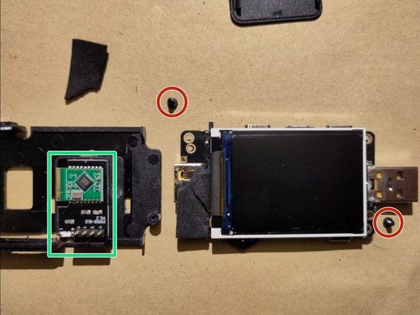
- Remove the two screws (redcircles) next to the USB-A connectors.
- Carefully bend the plastic (pink rectangle) on the menu select button to remove the PCB.
- If you have the FNB58B variant you should see the bluetooth module remain in the frame (green square).
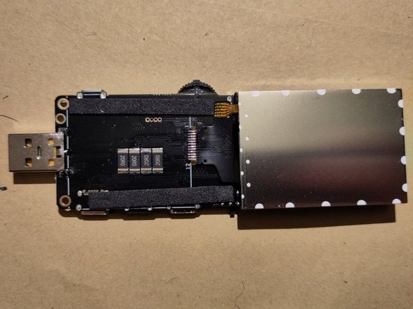
- Screen labelled "NFP200H-20A", could not identify further. Probably some standard TFT display with SPI/I2C.
- Backside main PCB:
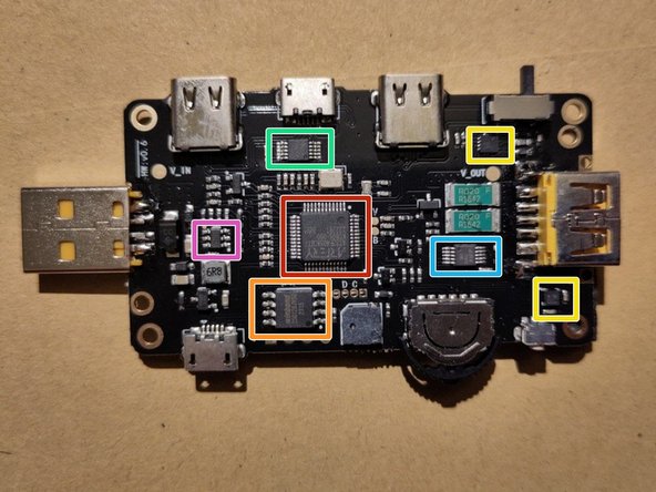
- Red square: Artery AT32F403A CGT7 (Main microcontroller) with orange square: W25Q128JV (128M-bit Serial Flash Memory with uniform 4KB sectors and Dual/Quad SPI)
- Blue square: 3PEAK TPA626 TPA626 (Bi-Directional Current and Power Monitor)
- Green square: RS2228 MCO7117 (High-Speed USB 2.0 (480-Mbps) 1:2 Multiplexer/Demultiplexer Switch). Probably to switch between the USB micro and -C inputs.
- Pink square: IC labelled IV7NS. I think it might be a MPS MP2451DT step-down converter. Probably to always provide the 3.3V logic-level voltage for the ICs.
- Yellow squares: could not identify. One (presumably) QFN14 labelled "UAAC CEH" and one with unknown form factor "WL5 J3".
- Bluetooth board: pogo-pins to make contact to main board and Tuya BEKEN BK3432