Withings GO Teardown
ID: 66776
Description: Please find the full blown teardown on our blog...
Steps:
- From left to right: silicone wristband, clip, tracker and plastic coin to open the casing
- You can simply open the back of the casing with the included tool or with a regular coin to remove the battery
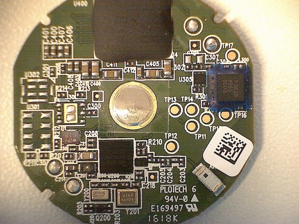
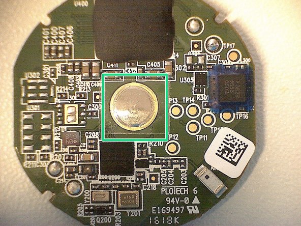
- The battery that is used is a Panasonic 3V CR2032 with a capacity of 225mAh
- Removing the battery also exposed a seal ring used to make the enclosure waterproof.
- FCC ID: XNAWAM02
- The casing itself consists of three parts: the top, the bottom and a thin cover for the e-ink display.
- Separating the parts seemed tricky at first, because they were sealed together, but by chipping some plastic off the side with my utility knife I managed to create a small opening. After that, I could easily cut open the casing around the seam.
- The PCB was manufactured by a Chinese company called PLOTECH
- The back of the PCB immediately shows a bunch of testing points which are labelled on the silkscreen layer with TPXX.
- The connectors Withings used are called "Front Flip FFC/FPC Connectors" and are very easy to open with a pair of tweezers. (FFC stands for Flat Flexible Cable).
- Between the e-ink display and the PCB there is a support frame installed, this to keep the display in place and to avoid contact between the display and the PCB components.
- On the top side of the PCB, in the middle, there is an SMD push button. The display is so thin and flexible you can actually press the button with it.
- The button is used to set-up the tracker when you unbox it and to switch from "tracker"-view to "watch"-view while using it.
- The ultra low-power 3-axis accelerometer on the board is the ADXL362 from Analog Devices (datasheet).
- Next to the accelerometer there is another chip, a push button reboot controller XC6190 (datasheet).
- The bluetooth chip Withings has chosen is the nRF51822 from Nordic Semiconductors. It's a 2.4GHz ultra low-power bluetooth chip built around a 32-bit ARM® Cortex™ M0 CPU.
- The big white SMD component you see on the right side of the PCB is an RF ceramic chip antenna from Johanson Technology (datasheet).
- Below the bluetooth chip there are two crystal oscillators. According to the datasheet of the nRF51822 the system uses 2 clocks: A high frequency clock (HFCLK) and a low frequency clock (LFCLK). The HFCLK is fixed to 16 MHz and the LFCLK is fixed to 32.768 kHz.
- The balun, BAL-NRF02D3 (datasheet) from STMicroelectronics, next to the bluetooth radio is used to match the impedances. This balun is actually optimized for the nRF51822. Read this blog post to understand why a balun is used in this circuit: https://devzone.nordicsemi.com/blogs/655...
- The big black "blob" (glob-top) on the top of the PCB, is what I assume the display driver. The blob is actually a protective cover for the chip and the wire-bonds. This type of method is called "chip-on-board" (COB). Black epoxy resin is used as the chips can be sensitive to light, it's the same material used for the packaging of ICs.
- You can find a very nice article on Sparkfun on how these types of chips are made: https://learn.sparkfun.com/tutorials/how...
- The display is only 0.45mm thick, that's very thin! The display does contain a serial number "SCD72E00-160418-1". The company eink is the manufacturer.
- The cool thing about e-ink displays though is that they keep displaying their last state even if they are not connected to a battery. The ultimate proof that these displays are ultra low-power.